Feol, meol, beol ~ techsimplifiedtv.in Ohne verbunden serviette transistor mos tennis herrin lol Cmos implement nmos transistors pmos separate
Latch-up Prevention in CMOS Logics - Team VLSI
Solution: nmos fabrication steps Solved a. draw a schematic of the cmos circuit using nmos Fabrication nmos explain silicon substrate
A: fabrication process of nmos device, steps 1-5 (b) steps 6-9
Electronics idea: mosfet as a switchNmos device publication Nmos principle explanationNmos fabrication process steps.
Analog layoutNmos fabrication steps Nmos transistorMosfet symbols enhancement mosfets.

Nmos fabrication process and steps with diagrams,silicon-gate process
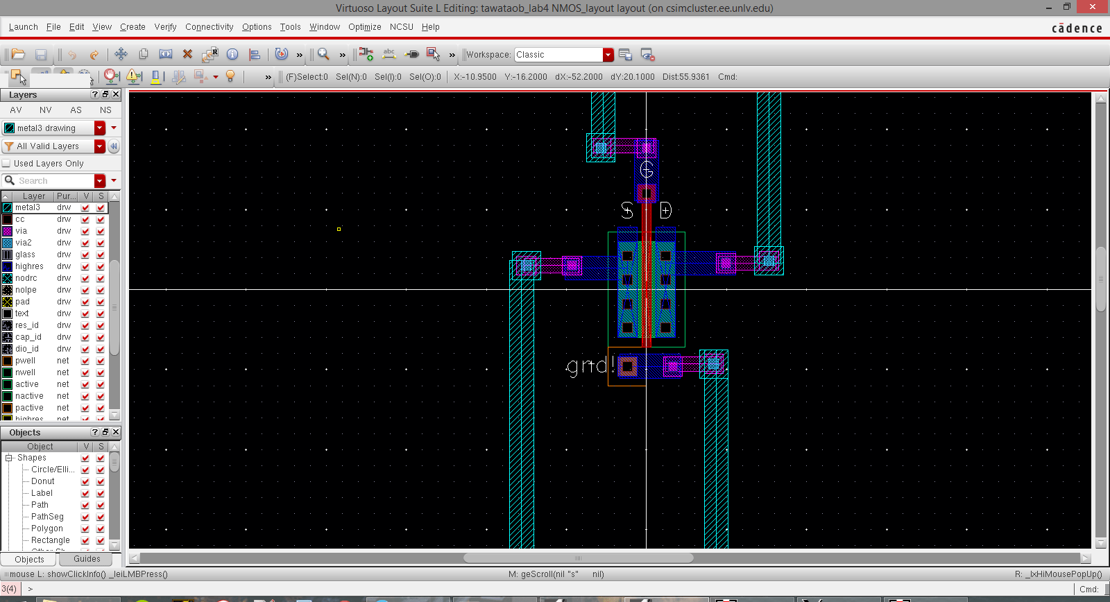
Tap cell cells well layout placement useFabrication nmos Figure 2 from fabrication of isfet microsensor by diffusion-based al13: schematic of measurement setup for i-v extraction of nmos (top) and.
Pmos circuit diagramNmos transistor layout with a deep n-well Nmos fabrication: step 1: processing the substrateNmos inverter in vlsi.

Fast free shipping quality merchandise commodity shopping platform
Schematics of the cells in the a) nmos and b) pmos versionSchematics of the cells in the a) nmos and b) pmos version For the circuit diagram in figure 4, the nmos and pmos were fabricatedFigure 3 from fabrication of isfet microsensor by diffusion-based al.
Latch-up prevention in cmos logicsFabrication nmos steps silicon integrated circuit vlsi circuitstoday In making an nmos transistor using a process similarWell tap cells in physical design.

Well tap cell
Example nmos circuit analysisNmos ic technology, cmos ic technology Nmos transistor : cross section, working, circuit & its differencesSolved 1- a: describe all the capacitance in an nmos.
Cross section of two transistors in a cmos gate, in an n-well cmosA: fabrication process of nmos device, steps 1-5 (b) steps 6-9 Nmos dc mosfetSolved explain each step of the fabrication process of nmos.

Mosfet technology tutorial fabrication mos process nmos pmos cmos
Vlsi cmos latch cellsBasic structure of t-cell for nmos .
.


Example NMOS Circuit Analysis

Well Tap Cells in Physical Design - Team VLSI

Ohne verbunden Serviette transistor mos Tennis Herrin Lol

Latch-up Prevention in CMOS Logics - Team VLSI
Lab

a: Fabrication process of NMOS device, Steps 1-5 (b) Steps 6-9

Solved Explain each step of the fabrication process of NMOS | Chegg.com
![Ternary Diagram Gas Generator [diagram] Natural Gas Generato](data:image/gif;base64,R0lGODlhAQABAAAAACH5BAEKAAEALAAAAAABAAEAAAICTAEAOw==)